
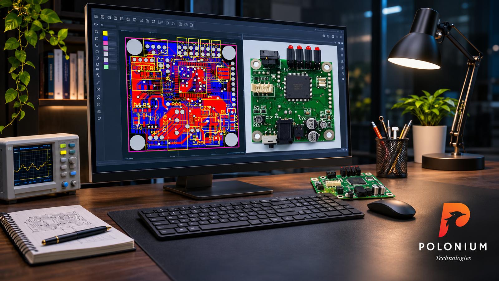
A good schematic means little if the board fails in real life, and PCB layout is the step that makes the board work. Layout places each part and draws the copper tracks that link them. This guide shows you each step, from the board outline to the final files.
You will learn how to place parts with sense and route tracks with care. Next, you will see how to plan power, ground, and heat. By the end, you will know how to check the board and send it to build.
This guide uses plain words and short steps. You need no deep math to follow it. If you have a schematic, PCB layout gives you the path from that drawing to a board you can hold.
What is PCB layout?
PCB layout is the physical build of a circuit board. You place each part on the board outline and draw the tracks that link them. The layout sets the board size, the layer count, and the track widths. A neat PCB layout keeps signals clean and parts cool.
Good PCB layout starts with the schematic in hand. First, read the schematic and note the hot parts and tall parts. Then plan the board size and the part spots. A clear plan at this stage makes each later step easy.
Start with the board outline and stack-up
Draw the board outline before you place a part. Note the case size, the mount holes, and the keep-out zones. A board that fits the case saves a full rebuild later. Keep the outline simple so the factory can cut it with ease.
Pick the layer count next, and let the circuit set it. A simple board needs two layers, while a fast board needs four or more. More layers cost more, but they give clean power and ground planes. So pick the count that fits the job and the budget.
Place the parts with sense
Place the big parts first, then fill the gaps with small parts. Put the MCU near the centre and the connectors at the board edge. Keep the crystal close to the MCU so the clock stays clean. A neat placement shortens the tracks and cuts noise.
Group parts by function as you place them. Keep the power block in one spot and the radio block in another. Leave room near hot parts so heat can spread. Then check the part heights in 3D to spot clashes early.
Route the tracks in PCB layout
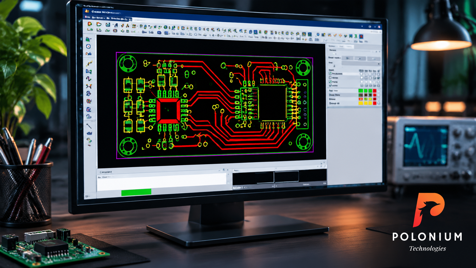
Route the power tracks first and make them wide. A wide track carries more current and stays cool. Keep signal tracks short and straight so signals stay clean. Avoid sharp bends that can trap acid in the etch.
Route the fast signals next, and keep them away from noisy parts. Pair the data lines that must run as one. Add a ground plane below them to cut noise. Then run design rule checks to catch tight gaps.
| Step | What you do | Output |
|---|---|---|
| Outline | Draw the board shape and layers | Board outline |
| Place | Set each part in its spot | Placed board |
| Route | Draw the copper tracks | Routed board |
| Check | Run design rule checks | Clean files |
| Build | Send files to a factory | Bare board |
Plan power, ground, and heat
Power needs a clear path from the input to each part. Use wide tracks or copper pours for the main rails. Add caps near each chip to smooth the supply. A clean supply keeps the circuit calm and stable. A cool board lasts long in the field.
Heat needs a path out of the board as well. Give hot parts copper pours and space to breathe. Add vias to move heat to the far side. Then check the hot spots with a thermal view before you build.
Check the board before you build
Run design rule checks on the full board. The checks flag tight tracks, weak clearances, and missing links. Fix each fault the check finds before you order boards. A clean check saves a costly rebuild.
Ask a peer to review the PCB layout with fresh eyes too. A second pair of eyes spots tight tracks and weak power paths. The review also checks the part footprints and the board edge. So run a review before you send the files out. A clean board ships with trust.
Common PCB layout mistakes
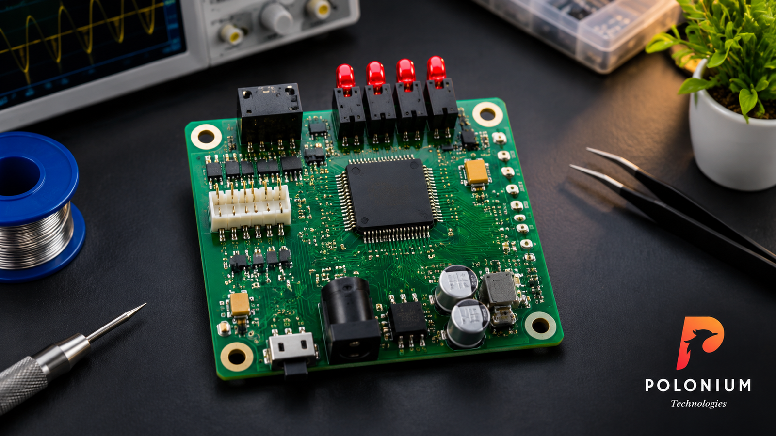
New designers repeat the same faults in PCB layout. They crowd parts close with no room for heat. Next, they route long tracks with no ground plane. They skip the design rule checks, and faults reach the factory. In short, small faults in the plan grow into big faults in the board.
A design review stops most of these faults. A second pair of eyes spots tight tracks and weak power paths. The review also checks the part footprints and the board edge. So run a review before you send the files out. A one-hour review can save a full rebuild.
Common questions about PCB layout
Q: How long does PCB layout take?
A: It depends on the part count and the board size. Simple boards take days. Complex boards take more time.
Q: Do I need a schematic before PCB layout?
A: Yes. The layout builds from the schematic. Without it, the layout team has no circuit to build.
Q: What files come out of PCB layout?
A: You get Gerber files, a drill file, and a bill of materials. The factory needs all of them to build your board.
PCB layout turns a schematic into a board you can hold. Place parts with sense, route tracks with care, and check each step. Polonium Technologies lays out PCBs for teams around the world. Share your schematic, and the team will turn it into a board you can test. Visit the Services page (https://poloniumtechnologies.com/services/) to start, or send an inquiry through the Contact page (https://poloniumtechnologies.com/contact/).