
A client walks in with an old board and no files. The board works, but no one has the schematic or the layout. PCB reverse engineering solves this exact problem. It reads the board and rebuilds the design from it.
In this guide, you will learn what PCB reverse engineering means. You will see the steps, the tools, and the risks. You will also learn when it makes sense and when it does not. By the end, you will know how an old board turns into a fresh design.
This guide keeps things simple. You need no engineering degree to follow it. We use plain words and short steps. If you own an old board, this guide shows you the path to a new one.
What is PCB reverse engineering?
PCB reverse engineering means reading a finished board and rebuilding its design. An engineer studies the board, the parts, and the copper tracks. Then the engineer draws a fresh schematic from what the board shows. The result is a design you can build, fix, and improve.
One rule comes first: only reverse-engineer boards you own or have the right to copy. A board may hold a design that belongs to someone else. Copying it with no right can break the law. So check the rights first, and work only on boards you own.
How PCB reverse engineering works
PCB reverse engineering runs in clear steps. First, the engineer photos the board from both sides. Next, the engineer notes each part and its value. Then the engineer removes the parts with care to see the tracks. After that, the engineer follows each track and writes the net list.
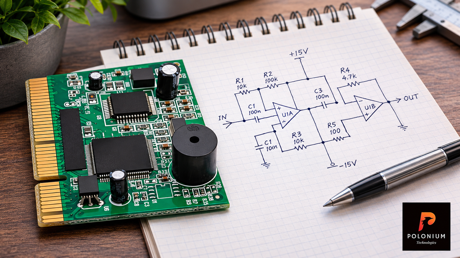
The net list feeds the schematic. The engineer draws each part and each link in the ECAD tool. Then the engineer lays out a fresh board from the schematic. The new board keeps the old circuit and fixes its weak spots. So the work ends with files you can build from.
| Step | What you do | Output |
|---|---|---|
| Inspect | Photo the board, note the parts | A full record |
| Remove parts | Take parts off with care | A bare board |
| Trace | Follow each copper track | A net list |
| Draw | Build the schematic | A new schematic |
| Rebuild | Lay out a fresh PCB | New Gerber files |
Tools for PCB reverse engineering
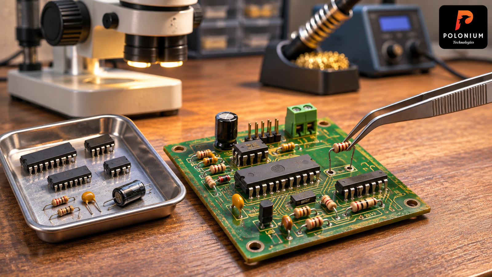
Simple tools do most of the work. A good camera records the board in fine detail. Next, a microscope shows small tracks and tiny part marks. A multimeter checks each link for breaks. These tools cost little, and they fit on a small bench.
Software helps too. The ECAD tool holds the schematic and the layout in one project. A photo tool lines up the top and bottom shots. In addition, a scanner can read the board layers in fine steps. So pick simple tools first, and add gear only when you need it.
When teams need PCB reverse engineering
Teams need PCB reverse engineering when the files are gone. A supplier may close, or an old drive may die with the design. The board still works, but no one can build a fresh one. In that case, reverse work brings the design back to life.
Repair teams use it too. An old machine breaks, and the spare board is gone from the market. Reverse work rebuilds the board so the machine runs again. It also helps teams upgrade an old product with new parts. So one old board can start a whole new product line.
Common risks in PCB reverse engineering
Reverse work has real risks. A wrong trace can flip a signal and break the circuit. Next, a missed part can change how the board acts. A wrong footprint can stop a part from fitting. So check each step twice, and test the new board with care.
Tests catch most faults before the board ships. Power the new board in small steps, and watch the current at each step. Compare each signal with the old board. If a signal looks wrong, trace it back to the schematic. A slow test saves a fast failure.
From an old board to a new design
A rebuilt design from PCB reverse engineering is more than a copy. The engineer can fix weak spots and add new parts. Next, the team can swap old parts for new ones that cost less. The new board can also gain features the old one lacked. In short, reverse work can upgrade the product, not just copy it.
Polonium Technologies takes on reverse work for teams around the world. Share your board and your goal, and the team will map the path. The team rebuilds the design and guides you to a tested board. Start with a short note about your board and what it must do.
PCB reverse engineering for repairs
Repair shops use PCB reverse engineering each day. A machine stops, and the maker no longer sells the board. The shop reads the old board and builds a fresh one. The machine runs again, and the client saves the cost of a new machine.
Upgrades work the same way. The team reads the old board and adds a new sensor or a new link. The new board fits the old case and the old mounts. So the product gains new life with no full redesign. That is the quiet power of good reverse work.
Common questions about PCB reverse engineering
Q: Is PCB reverse engineering legal?
A: It depends on the board and the rights. Only work on boards you own or have the right to copy. When in doubt, ask the owner first.
Q: How long does PCB reverse engineering take?
A: It depends on the board size and the part count. A simple board takes days. A dense board with many parts takes more time.
Q: Can you copy any board?
A: No. Some boards hold designs that belong to others. A good team checks the rights first and works only on boards you own.
PCB reverse engineering turns an old board into a fresh start. You do not need the lost files to move ahead. You need a clear record, a neat schematic, and a test plan. Polonium Technologies can rebuild your board and guide you to a tested design. Need the board assembled too? We get PCBA done from China. Visit the Services page (https://poloniumtechnologies.com/services/) to start, or send an inquiry through the Contact page (https://poloniumtechnologies.com/contact/).