
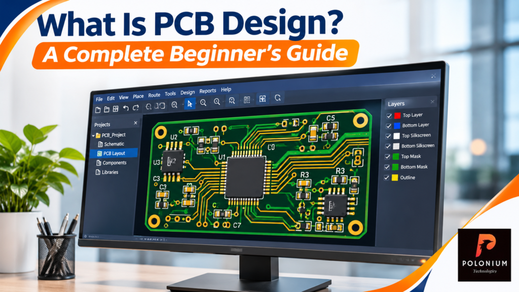
Every phone, laptop, and smart gadget hides a circuit board. That board links all the parts and makes the device work. PCB design is the craft that plans that board. It turns an idea into files, and a factory builds the board from them.
In this guide, you will learn what PCB design means and how it works. You will meet the two main steps: the schematic and the layout. Next, you will see the tools, the files, and the common faults. By the end, you will know how a board moves from an idea to a real product.
This guide keeps things simple. You need no engineering degree to follow it. We use plain words and short steps. If you have a product idea, this guide shows you the path from that idea to a working board.

What is PCB design?
PCB design is the plan for a circuit board. An engineer draws the schematic first, and then lays out the board. The schematic shows how each part links to the rest. After that, the layout sets the board size, the part spots, and the copper tracks. Those files tell a factory how to make the bare board.
Good PCB design needs care. Track width, part spacing, and heat all shape the result. A small fault in the plan can break the whole board. So a skilled designer checks the layout with design rule checks before the files go to the factory.
PCB design starts with a schematic
The schematic is the first step in PCB design. It is a drawing that shows the circuit as symbols and lines. Each symbol stands for a part, and each line stands for a link. The schematic does not show the board size or the part spots. It shows the logic: what links to what, and why.
A clear schematic saves hours later. It helps the layout engineer place parts with sense. It also helps the test team find faults fast. So spend time on the schematic, and keep the nets neat and named. A tidy schematic makes the whole job smooth.
From schematic to PCB layout
After the schematic, PCB design moves to the layout. The engineer places each part on the board outline. Big parts go first, and small parts fill the gaps. Then the engineer draws the copper tracks that link the parts. Each track must be wide enough for its current.
A good layout also plans for heat and power. Hot parts need space and copper pours to cool down. Power tracks need more width than signal tracks. In addition, a ground plane cuts noise and keeps signals clean. So plan the heat path and the power path from the start.
What tools do PCB designers use?
PCB designers work in ECAD tools. Altium Designer leads the pro market, and KiCad leads the free tools. Both tools link the schematic and the layout in one project. A change in the schematic flows straight into the layout. That link saves time and cuts errors.
A good tool also shows the board in 3D. You can see part heights and clashes before you order the board. In addition, the tool runs design rule checks for spacing and track width. These checks catch faults while they are cheap to fix. First, pick a tool that fits your budget and your team.

Common PCB design mistakes
New designers repeat the same faults. They draw tracks too narrow for the current. Next, they crowd parts close with no room for heat. They skip the ground plane, and noise creeps into the signals. In short, small faults in the plan grow into big faults in the board.
A design review stops most of these faults. A second pair of eyes spots tight tracks and weak power paths. The review also checks the part footprints and the board edge. So run a review before you send the files out. A one-hour review can save a full rebuild.
How to start your first PCB design
Start your first PCB design with a small idea. Pick a simple circuit, like a sensor board or a blinking LED board. Draw the schematic, and keep each net neat and named. Then place the parts, route the tracks, and run the design rule checks. Fix each fault the check finds, and your files will be clean.
When the files are clean, share them with a factory or a design team. The team checks the files and guides you to the next step. Polonium Technologies designs PCBs for teams around the world. Share your idea, and the team will turn it into a board you can test.
| Step | What you do | Output |
|---|---|---|
| Idea | Draw the schematic | Schematic file |
| Layout | Place parts and route tracks | Gerber files |
| Check | Run design rule checks | Clean files |
| Build | Send files to a factory | Bare board |
Common questions about PCB design
Q: How long does PCB design take? A: It depends on the board size, the part count, and the circuit. Simple boards take days. Complex boards take more time.
Q: Do I need costly software to start PCB design? A: No. KiCad is free, and it handles most small boards. You can move to Altium later when your work grows.
Q: What files do I get after PCB design? A: You get Gerber files, a drill file, a bill of materials, and a pick-and-place file. The factory needs all of them to build your board.
Good design turns an idea into a board you can hold. You do not need a big team to start. You need a clear schematic, a neat layout, and a review before you build. Polonium Technologies can guide you from the first sketch to the final files. Need the board assembled too? We get PCBA done from China. Visit the Services page to start, or send an inquiry through the Contact page.
Further reading: IPC and All About Circuits.